Switch/button/LED demo for Arty-A7, but using AXI (part 1)
After getting a Digilent Arty-A7, I quickly found this programming tutorial. It is a very simple demo where the switches and push buttons are OR’ed into the LEDs. The implementation is a single Verilog source file:
module sw_btn_led(
    input [3:0]sw,
    input [3:0]btn,
    output [3:0]led
    );

    assign led = sw | btn;

endmodule
Very simple and sufficient for the goal of explaining how to program the board with Vivado tools, but I wanted to know how to do this “from scratch”. I have the board support files installed and after starting a new project, selecting the Arty-A7 as the target platform, I start with creating a new block design. Under the “Board” tab, you’ll find a list of all the connections that the board supports:
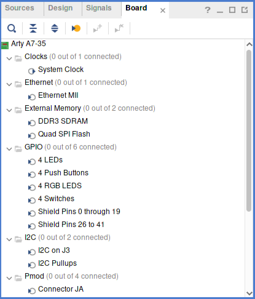
Dragging for example the “4 Push Buttons” onto the block diagram, will result into this:
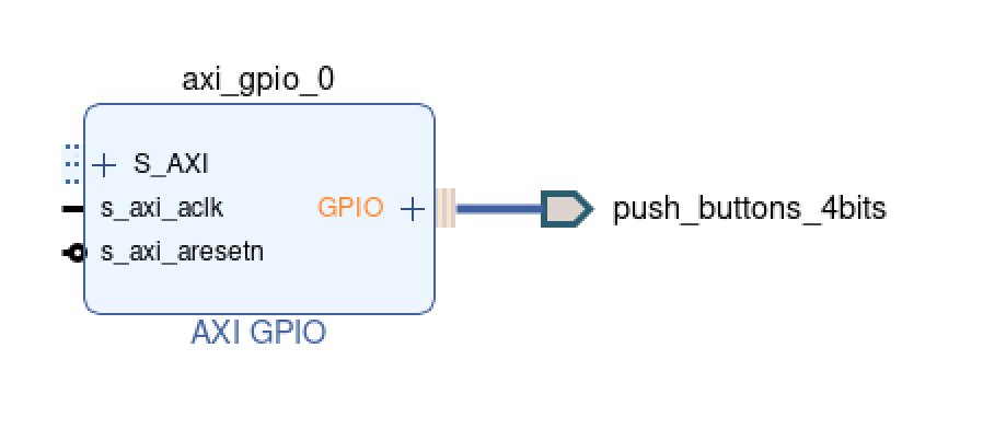
Vivado has automatically added (or prompts you to add, depending on your settings) an “AXI GPIO” block. This is because
Digilent has specified in their board support file that this peripheral is preferably used with a “AXI GPIO” block (see
board.xml in the board support package):
<interface mode="master" name="push_buttons_4bits" type="xilinx.com:interface:gpio_rtl:1.0" of_component="push_buttons_4bits" preset_proc="push_buttons_4bits_preset">
  <description>4 Push Buttons</description>
  <preferred_ips>
    <preferred_ip vendor="xilinx.com" library="ip" name="axi_gpio" order="0"/>
  </preferred_ips>
  <port_maps>
    <port_map logical_port="TRI_I" physical_port="push_buttons_4bits_tri_i" dir="in" left="3" right="0">
      <pin_maps>
        <pin_map port_index="0" component_pin="push_buttons_4bits_tri_i_0"/>
        <pin_map port_index="1" component_pin="push_buttons_4bits_tri_i_1"/>
        <pin_map port_index="2" component_pin="push_buttons_4bits_tri_i_2"/>
        <pin_map port_index="3" component_pin="push_buttons_4bits_tri_i_3"/>
      </pin_maps>
    </port_map>
  </port_maps>
</interface>
The AXI GPIO block is not very complicated, and the AXI protocol is also manageable for the simple read/write operations that we are going to for AXI GPIO (streaming and burst data transfers with multiple AXI master and slave modules on the bus quickly gets really complicated, as this blog post explains much better than I can). So, let’s see if we can redo the button/switch/led demo with AXI GPIO.
Step 1: A simple AXI master
First we create a simple AXI master in VHDL. This module will read the states of the buttons and switches and drive the LEDs accordingly.
In the AXI specification you can find which inputs and ouputs are required for the “Lite” version of the AXI protocol, which supports only simple read and write operations. Here is the entity specification with all the required inputs and outputs specified:
entity axi_led_ctrl is
    Port (
            -- General
            m_axi_aclk      : in std_logic;
            m_axi_aresetn   : in std_logic;

            -- Write address channel
            m_axi_awready   : in std_logic;
            m_axi_awvalid   : out std_logic;
            m_axi_awaddr    : out std_logic_vector(31 downto 0);
            m_axi_awprot    : out std_logic_vector(2 downto 0);

            -- Write data channel
            m_axi_wready    : in std_logic;
            m_axi_wvalid    : out std_logic;
            m_axi_wdata     : out std_logic_vector(31 downto 0);

            -- Write response channel
            m_axi_bvalid    : in std_logic;
            m_axi_bready    : out std_logic;

            -- Read address channel
            m_axi_arready   : in std_logic;
            m_axi_arvalid   : out std_logic;
            m_axi_araddr    : out std_logic_vector(31 downto 0);
            m_axi_arprot    : out std_logic_vector(2 downto 0);

            -- Read data channel
            m_axi_rready    : out std_logic;
            m_axi_rvalid    : in std_logic;
            m_axi_rdata     : in std_logic_vector(31 downto 0)
         );
end axi_led_ctrl;
Add a new VHDL source file to the project. You can specify the inputs and outputs in the wizard, or just copy the above into an empty source file.
In this first version, I’m just going to have the module turn some LEDs on continuously, and in a future post implement something more advanced. Add this below the interface specification:
architecture Behavioral of axi_led_ctrl is
    signal clk  : std_logic;
    signal rstn : std_logic;
begin

    -- Map general signals
    clk <= m_axi_aclk;
    rstn <= m_axi_aresetn;

    -- Default protection flags
    m_axi_awprot <= "000";
    m_axi_arprot <= "000";

    process(clk, rstn) is
    begin
        if rising_edge(clk) then
            if rstn = '0' then
                m_axi_awvalid <= '0';
                m_axi_wvalid <= '0';
                m_axi_arvalid <= '0';
            else
                -- Write to LEDs
                m_axi_awvalid <= '1';
                m_axi_awaddr <= x"40010000";  -- address of GPIO1
                m_axi_wvalid <= '1';
                m_axi_wdata <= x"0000000B";  -- LED3, 1 and 0 on

                -- No reading
                m_axi_arvalid <= '0';
            end if;
         end if;
     end process;


end Behavioral;
Note the address of GPIO1; we’ll come back to that later.
Here you can find the entire VHDL source file for convenience.
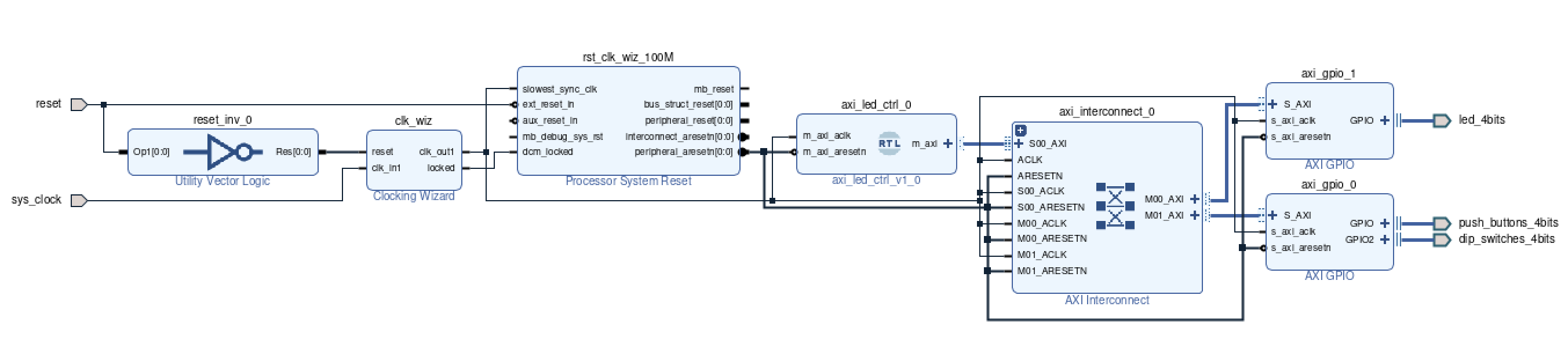
Step 2: Block design
Create a new block diagram and drag the “4 Push Buttons”, “4 Switches” and “4 LEDs” onto the canvas, as well as our master controller. Vivado will help with auto routing and connections, and will (should) ask to add the following components (your mileage may vary, since a lot seems to depend on the order in which you add things to the block design):
- AXI interconnect
- Clocking wizard
- Processor System Reset
It should also connect to the reset button and the board’s sys_clock. The reset button is active low, so Vivado will
also add an inverter to connect the reset to the clocking wizard, which has an active high reset.
In the end, the block design should look like this:
Open the address editor to check which addresses Vivado assigned to which GPIO block. As you can see, I have both the
push buttons and the switches on axi_gpio_0 and the LEDs on axi_gpio_1. Here is my address map:
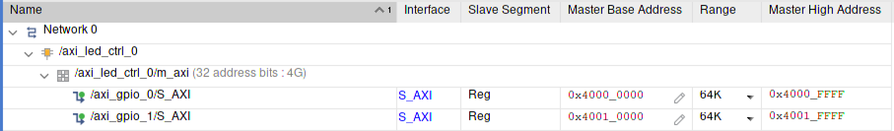
Note that the LEDs are at 0x40010000, which corresponds to the address in the AXI master.
Step 3: Synthesize the design
You cannot synthesize the block design directly. Create a HDL wrapper first and then follow the design flow: synthesis, implementation and bitstream generation. Finally, program the device and see LED3, LED1 and LED0 come on.
In a future post, I’ll build forward on this and actually do something with the switches and push buttons.