Switch/button/LED demo for Arty-A7, but using AXI (part 2)
In a previous post I optimistically set out to reproduce the switch/button/LED demo from Digilent, but using AXI. I quickly had some LEDs lighting up, but reading out the push buttons and the switches proved to be a bit more difficult than I anticipated. Probably because I’m not using VDHL and AXI on a daily (or any) basis, so this was a lot of learning. The things I will outline below are maybe obvious to the experts, but as it was not obvious to me, I’m imagining it is not obvious to other beginners either, so hopefully this is useful.
Why it took me so long to make a simple demo
AXI is hard
Actually, it is not that hard in theory. The protocol is pretty well documented (the specification can be found here) and the principle is straightforward:
- There are five channels: write address, write data, write response, read address and read data.
- All five channels use the same handshake protocol,
which boils down to: the originator asserts
VALIDwhen the data is valid, and the receiver assertsREADYto indicate the completion of the transfer.
To write data somewhere, the sequence of events is roughly as follows:
- The AXI master first uses the write address channel to indicate where the data should go to.
- Then, the data is put on the write data channel
- After the data transfer is complete, the AXI slave responds with the result (success, failure, etc.) on the write response channel.
For reading data from somewhere, it is more or less similar, except that there is no read response:
- The AXI master uses the read address channel to indicate where to read from.
- The slave puts the data on the bus and waits for the master to complete the transaction.
Now, the difficulty (at least for me as unexperienced hobbyist) is that all kinds of things can happen at the same time if your not careful. ARM explains in detail the dependencies between the various handshake signals, but then it is still easy to mess things up. Fortunately, someone way smarter than me wrote an excellent article on AXI handshaking rules and some basic principles that one should obey in order not to mess things up. Recommended reading.
Simulation is hard
Vivado has a nice simulation suite built in, and you can make nice test benches for your IP cores to verify that they work as intended. Of course, this requires that you apply the correct stimuli at the correct times. Only when I found out about Xilinx Integrated Logic Analyzer I learned that my simulation did not correspond with what was happening in reality, explaining why my design worked fine when I simulated it but did nothing when flashed on the board. For those of you who are also unfamiliar with ILA: it basically allows you to monitor signals on the board in real-time. It can hook up directly to the AXI bus, or to individual signals. You need to specify useful triggers to make sure that you see what you need to see, but once you get the hang of it, it is extremely useful.
Logic is hard
If you are a “regular” programmer like me, FPGA programming is hard. You need to think about how signals combine and interact and forget about the order in which you wrote things down. This is a different mindset that I find hard to adopt. Especially when clocked signals are used, I keep getting surprised.
For example, if the following procedure is used in a clocked process, signal_out will change the clock cycle after
some_condition becaume true.
procedure myProcedure(...) is
begin
    if some_condition = false then
        signal_out <= '1';
    else
        signal_out <= '0';
    end if;
end procedure;
However, in the following example, signal_out will change immediately when some_signal becomes 1, even if
some_condition is false (again: probably obvious to some, not to me):
procedure myProcedure(...) is
begin
    if some_condition = false then
        signal_out <= '1';
        if some_signal = '1' then
            signal_out <= '0';
        end if;
    else
        signal_out <= '0';
    end if;
end procedure;
This tripped me up in implementing the AXI handshakes, because I initially used the first version in handling the AXI
channel transfer, which resulted in the valid signal (signal_out) to be asserted one clock cycle too long, which
locked up the GPIO IP. This is where the ILA came in handy, because with it I could see the write response indicating
what I had done wronge. Live and learn.
Implementation of the AXI protocol
With that out of the way, let’s move forward with the implementation. The entire VHDL code can be found here.
State machine
I figured the most straightforward way to implement the AXI protocol correctly is by implementing a state machine that does one thing at the time. I ended up with seven states:
Idle: do nothingReadSwitchAddr: put the address of the switches on the read address channelReadSwitchData: read the switch states via the read data channelReadButtonAddr: put the address of the push buttons on the read address channelReadButtonData: read the button states via the read data channelWriteLed: write the desired LED state on the write data channelNoOp: placeholder that I will explain later
type state_t is (Idle, ReadSwitchAddr, ReadSwitchData, ReadButtonAddr, ReadButtonData, WriteLed, NoOp);
I didn’t bother to make separate states for the write address channel and the write response, since I’m always writing to the same address. I didn’t handle the write response in a separate state either, since if writing to the LEDs failed I had no other way to signal the error anyway.
Handshakes
Since all channels use the same handshake protocol, I figured it would be a good idea to make a procedure for it. In this way, once I had one channel correctly implemented the rest would be easier. The procedure I came up with is the following:
procedure waitXferComplete(
    signal valid : out std_logic;
    signal ack : in std_logic;
    variable complete : inout boolean;
    signal state : inout state_t;
    constant next_state : in state_t
) is
begin
    if complete = false then
        valid <= '1';
        state <= state;
        if ack = '1' then
            valid <= '0';
            complete := true;
            if next_state /= NoOp then
                state <= next_state;
            end if;
        end if;
    else
        valid <= '0';
        state <= state;
    end if;
end procedure;
The ack signal is defined as x_valid and x_ready (for various x). As soon as the transfer is complete, it
deasserts the valid signal and transitions to the next state. I pass in the state of the state machine that should be
next once the transfer is completed. I abuse the NoOp state so I can run multiple instances of this procedure in
parallel with only one triggering a state transition (I do this in the WriteLed state).
Here’s a short version of how to use it:
arack <= arvalid and M_AXI_ARREADY;
-- ...
process(clk, resetn, ..., arack, ...) is
    -- ...
        variable arcomplete : boolean := false;
    -- ...
    begin
        if rising_edge(clk) then
            case state is
                -- ...
                when ReadSwitchAddr =>
                    M_AXI_ARADDR <= x"40010000";
                    waitXferComplete(arvalid, arack, arcomplete, state, ReadSwitchData);
-- ...
end process;
Note that in the read data state, the ready signal takes the place of the valid signal, as the roles of master and slave are reversed for the handshake.
Combinatorial logic
I choose to keep the logic of mapping switch and button states to LED states outside the process:
M_AXI_WDATA <= switch_state or button_state;
The registers with the switch and button states are read in a process separate from the state machine:
process(clk, state, rack, M_AXI_RDATA) is
begin
    if rising_edge(clk) then
        if rack = '1' and state = ReadSwitchData then
            switch_state <= M_AXI_RDATA;
        elsif rack = '1' and state = ReadButtonData then
            button_state <= M_AXI_RDATA;
        end if;
    end if;
end process;
Putting it all together
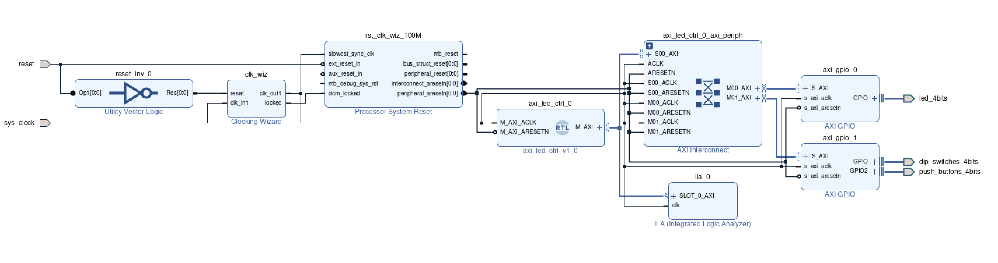
For reference, here is the entire block diagram. It should have been the same as the one posted in part 1, but in frustration I started over from scratch and as a result some details changed (in particular which peripheral is connected to which GPIO block). I also added the ILA.
I set a breakpoint in the ILA interface to trigger on a specifc value on the write data channel, corresponding to two
switches active and one push button (0xd). This allowed me to trigger the ILA with the push of a button, allowing me
to generate this trace (click for a larger version):
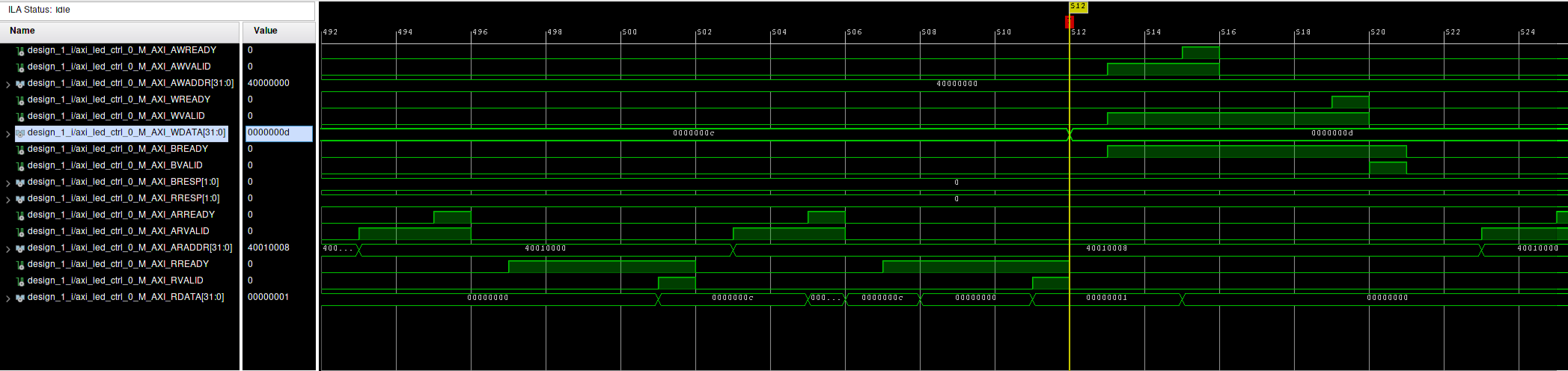
The trace shows an entire cycle of the state machine. On the left, we see two read cycles: one for the switches at
0x40010000 and one for the buttons at 0x40010008. Because the two registers with the switch and button states are
wired directly onto the write data signal, this is where the ILA triggers. On the right of the trigger we see from top
to bottom: the write address transaction, the write data transaction and the write response transaction (note how the
signals AWVALID and WVALID and BREADY are kept high due to my aforementioned laziness for not implementing
separate states). On the far right we see the Idle state and the beginning of the next read address state.
So, there it is: the switch-button LED demo with AXI. I’m sure there are things to comment on my VHDL abilities, so feel free to leave such comments in the gist (should be possible; it’s public).